AI Is Linking Semiconductor Design, Fab Operations and Inspection
NVIDIA argues that accelerated computing and AI can help semiconductor manufacturers manage growing design and fab complexity by linking simulation, digital twins, engineering support, robotics and inspection. Its account centers on a feedback loop: simulation and production data inform models, while inspection results feed back into them. NVIDIA reports chamber simulations up to 35 times faster and more than 96% accuracy in wafer-map defect classification, figures it presents as examples of the approach rather than measures of overall fab performance.
Simulation makes more design options practical
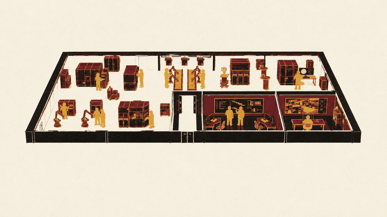
Demand for advanced chips is outpacing even ambitious forecasts, while the systems needed to design and manufacture them grow more complex. NVIDIA presents accelerated computing and AI as tools for addressing that complexity across semiconductor engineering and fab operations. Its overview spans processing equipment, wafer handling and material movement, metrology, inspection, process development and control, and fab operations—areas it depicts as connected within a fab digital twin.
The process begins with simulation. NVIDIA says its CUDA-X libraries use GPU acceleration across semiconductor engineering, turning computational bottlenecks into faster work in chip design and manufacturing. AI physics models learn from simulation and experimental data, helping engineers predict outcomes and explore more design options. NVIDIA reports that chamber simulations run up to 35 times faster.
The figure is specifically about chamber simulation, not a claim that every part of chip design or factory operations runs 35 times faster. The broader point in NVIDIA’s account is that faster simulation can help engineers examine more possibilities before committing changes to equipment or processes.
Digital twins extend that work beyond an individual simulation. NVIDIA describes them as shared virtual environments that bring equipment, processes and fab operations together. Teams can use that environment to optimize a system before introducing changes in the real world. A factory-floor rendering credited to Applied Materials illustrates the setting: rows of manufacturing equipment represented in a clean, virtual facility. The depiction places simulation within a view of factory operations, rather than treating it only as a design-stage calculation.
Agents connect model outputs to engineering and operating tasks
NVIDIA says AI agents bring together AI models and specialized skills to help engineers refine designs and processes. For operators, they can guide tasks such as predicting equipment issues and troubleshooting semiconductor test systems. The stated role is assistance with engineering and operational work; the source does not describe agents independently making production decisions.
The displayed workflow gives a more specific view of the components NVIDIA associates with agents. It names Nemotron and Kumo Anomaly Forecast under “Models,” NeMo and Omniverse under “Harnesses,” and predictive maintenance and diagnosis under “Skills.” The visual does not explain the technical boundaries among these categories, but it presents the agent workflow as a combination of models, harnesses and task-oriented skills—not as a single model acting alone.
That structure sits alongside the digital twin: the twin provides a shared virtual setting for equipment, processes and operations, while agents are described as helping people work with designs, processes and operational problems. NVIDIA’s overview connects these capabilities to a physical fab, where robots move materials, monitor equipment and perform complex tasks safely alongside people. The source describes this as part of a system connecting people, robots and processes; it does not specify which tasks are handled by agents versus robots.
A Pegatron interface shown on screen offers a concrete example of a simulated task. It pairs a 3D robot simulation with a chat about dispensing thermal paste onto a CPU. The interface lists a target volume of 500.0 microliters and a robot speed of 8.00 millimeters per second. In response to a request to dispense the paste, it reports a measured volume of 503.46 and says the volume goal has been met, with no anomaly detected. This is an example of a robot-related interface and status report, not evidence in the source of factory-wide performance.
Inspection turns production results into model feedback
In production, vision AI systems can perform quality inspection. NVIDIA says its Cosmos vision-language model has achieved over 96% accuracy in classifying wafer-map defects.
The displayed wafer-map interface shows a concentrated line of defects curving from the bottom left to the top right. Its response describes the pattern as non-random and indicative of a systematic rather than random cause. It identifies environmental or mechanical origins as possibilities and recommends targeted troubleshooting. The interface is an example of how a system might describe a visible pattern; the source does not establish a specific root cause for the wafer shown.
NVIDIA says each result feeds back into the models, creating a continuous cycle of learning and improvement. In its account, the cycle links several different kinds of work: simulation and experimental data inform AI physics models; digital twins let teams optimize equipment, processes and operations virtually; agents support engineers and operators; robots carry out physical tasks; and inspection produces results that return to the models. The claim is not that these stages remove the need for engineers and operators, but that AI tools connect their work across design, production and quality inspection.